

Crystalline silicon solar cells account for about 97% of the global market share. Reducing silver consumption is the key to meeting future production and cost targets. Copper is an ideal substitute for silver due to its low cost, abundant reserves and similar resistivity to silver. However, it has problems such as easy oxidation, diffusion into silicon and reduced minority carrier lifetime. This study reduces the degradation of copper metallized cells and improves the reliability of cells by optimizing the properties of copper paste.
Research Methods
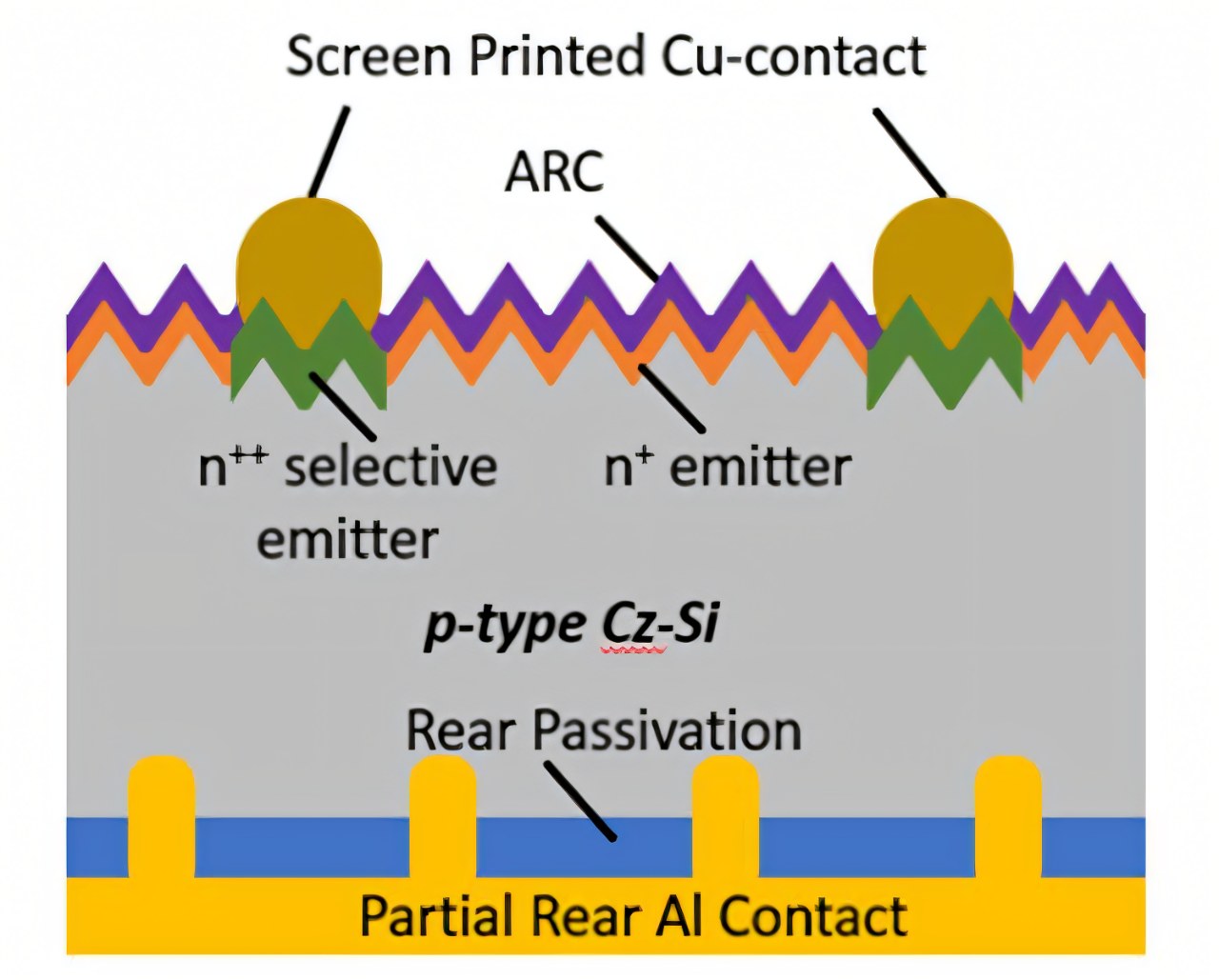
Schematic diagram of a selective emitter PERC cell
Cell preparation: Selective emitter PERC cells were prepared on monocrystalline p-type silicon wafers of M6 size (166 mm×166 mm). The front grid lines were screen-printed with copper paste, and the back side was aluminum (Al) contact with local contact openings.
Metalization process: Metallization is carried out in two steps. First, aluminum is printed on the back side of the silicon wafer, dried and sintered at about 751°C, followed by front grid line printing and sintering at about 630°C. At the same time, a reference cell with front silver printing was prepared using the same silicon wafer and a co-sintering temperature of 751°C.
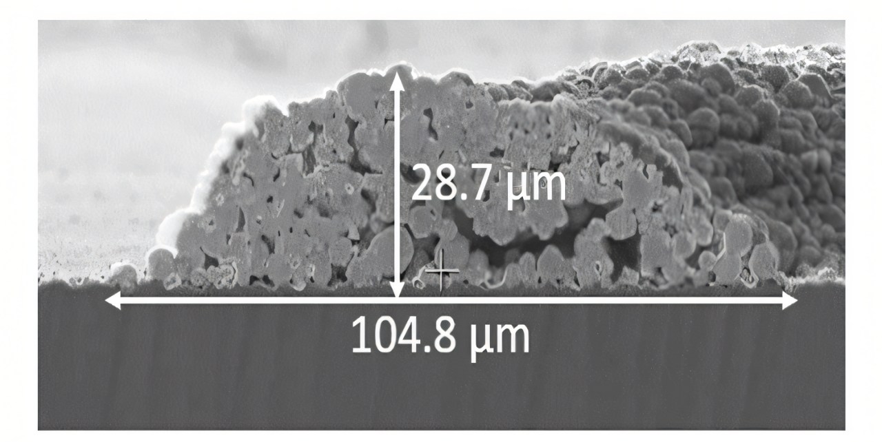
Scanning electron microscope image of a cross section of a copper finger
Copper paste properties: The optimized sintering peak temperature of the copper paste is about 630°C, and the resistivity is about 2-3×10^-5 Ω·cm. The cross-section of the copper finger was analyzed by scanning electron microscopy (SEM) and energy dispersive X-ray spectroscopy (EDS), and it was found that the copper finger width was about 100μm, the height was 28.7μm, and the aspect ratio was 0.27.

EDS analysis of different versions of copper paste
Initial version of copper paste: The initial version of copper paste has a thick oxide layer between copper and silicon. This thick oxide layer increases the series resistance of the solar cell, hinders the transmission of carriers, is not conducive to the improvement of solar cell performance, and leads to a decrease in the photoelectric conversion efficiency of the solar cell.
New version of copper paste: The oxide layer of the new version of copper paste is thinner. This structural change promotes carrier transmission and makes the current conduction inside the solar cell smoother. At the same time, the oxide layer is still thick enough to act as a barrier layer to prevent copper from diffusing into silicon, ensuring that the solar cell can still operate reliably and maintain good performance after 1500 hours of wet heat testing.
Electrical performance analysis

IV parameter distribution of a group of 100 PERC cells at different peak sintering temperatures
The 100 cells were divided into three groups, each corresponding to a different peak sintering temperature: 590°C, 610°C, and 630°C.
Voc: Voc has a slight increasing trend with increasing sintering temperature. This indicates that higher sintering temperature may help to increase the open circuit voltage of the solar cell.
Jsc: Jsc does not change much at different sintering temperatures, which indicates that the sintering temperature has little effect on the short-circuit current density.
FF: FF is the highest at a sintering temperature of 630°C, which indicates that the optimized sintering temperature can significantly increase the fill factor of the solar cell, thereby improving the overall efficiency.
Efficiency at different sintering temperatures: 590°C, the efficiency is low, the specific value is not given, but it can be inferred that it is lower than 19.25%. 610°C, the efficiency has increased, but it is still lower than the efficiency at a sintering temperature of 630°C. 630°C, the efficiency is the highest, reaching 19.25%.
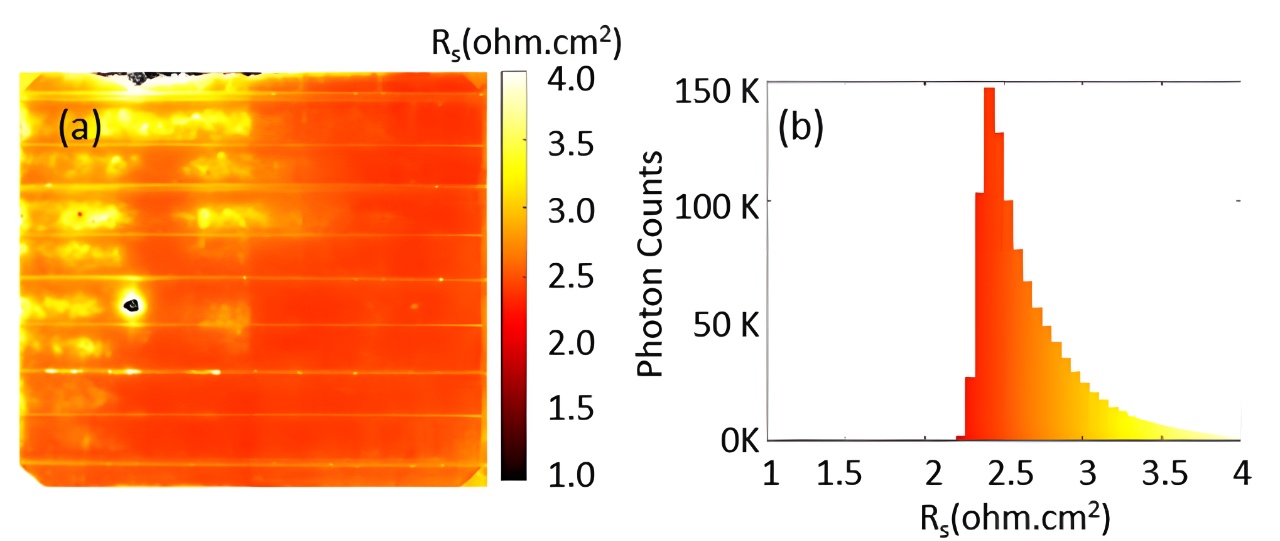
Series resistance distribution of copper metallized M6 size cell Series resistance
Series resistance(Rs): Color coding shows the series resistance values of different areas of the cell. Darker colors indicate higher series resistance, lighter colors indicate lower series resistance. Series resistance is an important parameter of solar cell performance, which affects the fill factor (FF) and overall efficiency of the solar cell. Higher series resistance leads to increased voltage drop in the solar cell, which reduces the output power of the solar cell.
Color coding: Quickly identify areas of high series resistance in the cell. These areas may be caused by non-uniformity of the copper fingers, non-uniformity of the oxide layer, or other manufacturing defects.
Reliability testing
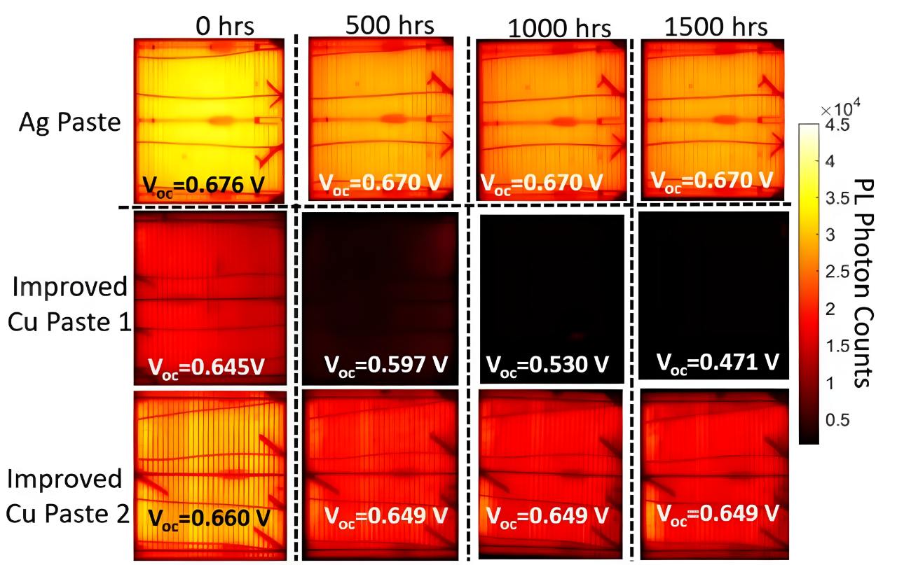
PL images before and after accelerated testing (85°C/85% humidity hot and humid environment)
PL images: The PL images show the luminescence intensity of the solar cell through color coding. The brighter the color, the better the solar cell performance, and the darker the color, the worse the solar cell performance. Initial state: Before the hot and humid test, the PL image shows that the solar cell emits brighter light as a whole, indicating good initial performance. Performance degradation: As the test time increases, the PL image shows that the luminescence intensity of the solar cell gradually decreases, especially in the crack area. This indicates that the solar cell has experienced performance degradation under hot and humid conditions, especially in the connection area. Improvement effect: After improving the copper paste properties, the PL image shows that the performance degradation of the solar cell is significantly reduced. This shows that the optimized copper paste plays an important role in improving the reliability of the solar cell.

Image observed by DLIT after damp heat testing
The cell was damp heat tested at 85°C and 85% humidity for 500 hours, and then DLIT tested at reverse bias (-3V, 0.3A):
DLIT image: Bright spots indicate the location of bypass diodes, which are defective areas in the cell that cause current to bypass the normal path, thereby reducing the performance of the cell.
Performance degradation: DLIT images show obvious bypass diodes in the cell after 500 hours of damp heat testing. This indicates that the cell has experienced performance degradation under damp heat conditions, especially in the copper/silicon interface area.
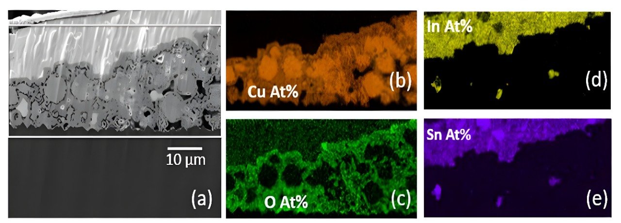
SEM and EDS analysis of copper contacts after ultrasonic welding
Cross-sectional SEM image: The bonding of the copper contact to the solder and the distribution of the solder on the copper contact can be observed. EDS analysis: The EDS analysis results provide information on the chemical composition of the welding area, and the distribution of elements such as copper (Cu), tin (Sn) and indium (In) can be observed. The uniform element distribution indicates that the elements are well mixed during the welding process, and there is no obvious uneven diffusion or element separation.
The optimized copper paste was found to achieve a cell efficiency of 19.25% at a sintering temperature of 630°C, and the cell still maintained good performance after 1500 hours of wet heat testing at 85°C and 85% humidity. These results show that copper paste has great potential in reducing the cost of photovoltaic production while meeting the requirements of high performance and high reliability.


 English
 español
 한국의
한국의


 IPv6 network supported