

The photovoltaic industry is developing rapidly and faces challenges in the long-term availability of key resources such as silver. The global photovoltaic industry consumed about 13% of the global annual silver production in 2022. Copper and aluminum are potential materials to replace silver. Copper is close to silver in conductivity, but there are technical challenges in applying copper-based metallization in high-temperature solar cell concepts (such as TOPCon), such as copper diffusion in silicon, oxidation, cross contamination, and long-term reliability of electrodes.
Screen-printed copper paste for metallization of TOPCon cells
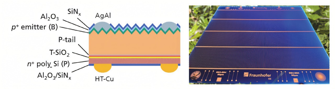
Schematic diagram of iTOPCon cell structure with screen-printed copper backside grid.
iTOPCon solar cell structure: including key parts such as n-type silicon substrate, tunnel oxide layer, passivation layer and metallization layer.
Copper back grid: screen-printed copper paste is used to form the metal grid on the back. This design is intended to replace traditional silver-based metallization to reduce the use of silver and improve the sustainability of the solar cell. Reasonable grid design can effectively reduce the series resistance of the solar cell and improve the photoelectric conversion efficiency.
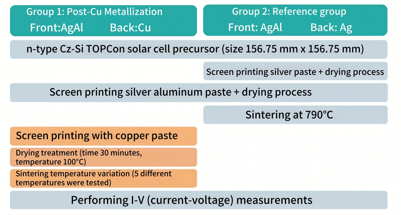
Flowchart of Experiment 1
Group 1: Metallization was performed using a standard front silver aluminum (AgAl) paste and screen printing was performed using a high temperature sintered copper paste on the back. The grid layout on the back includes 5 busbars (100 μm wide) and 160 fingerbars (80 μm wide). Group 2: Metallization was performed using a commercial silver paste on both the front and back. The front grid layout was the same as Group 1, and the back was a busbar-free layout, including 194 fingerbars (24 μm wide) and 12 dummy busbars (60 μm wide).
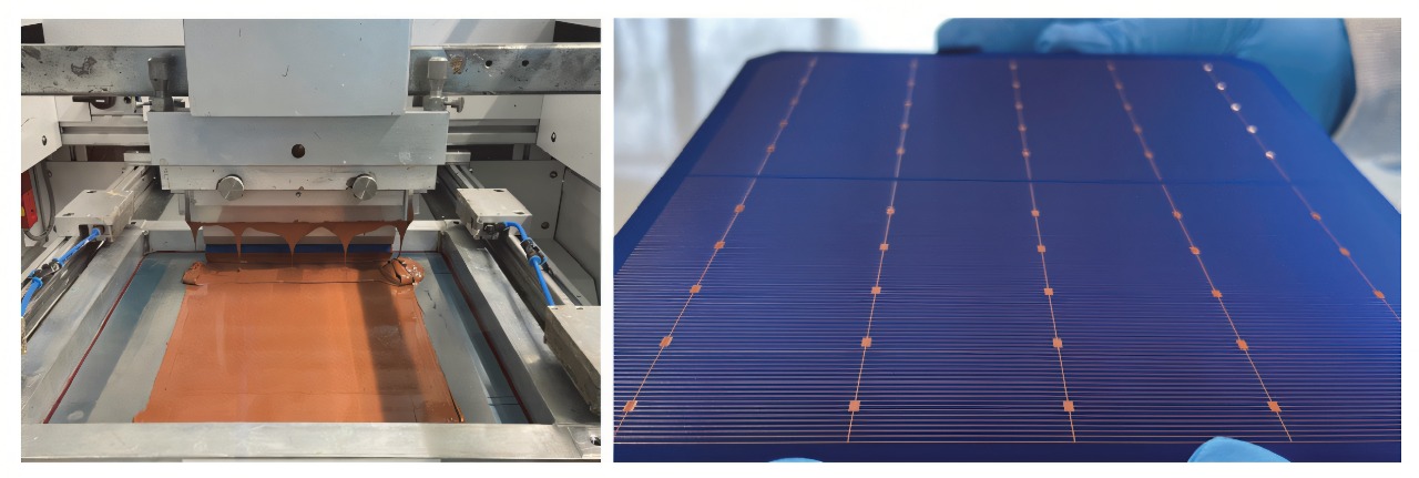
Screen printing of copper paste
Screen printing copper paste process: This is an important step in the experiment for the back metallization of TOPCon solar cells, where copper paste is applied to the solar cell by screen printing.
Copper grid layout of solar cell: The figure shows the copper grid layout formed on the TOPCon solar cell using screen printing technology. This grid layout is part of the solar cell metallization design and has a direct impact on the conductivity and efficiency of the cell.
Experimental results of Experiment 1

Confocal laser scanning microscope image of TOPCon cell after screen printing of copper paste
The image was measured by microscope, and the width of the copper paste finger stripes was clearly shown. After screen printing and sintering, the width of the finger stripes was about 130-150μm. The height of the copper paste finger stripes ranged from 20-25μm. The shadow effect of the finger stripes in the figure shows that a clear metallization pattern has been formed on the back of the solar cell. This shadow effect has a dual effect on the photoelectric conversion efficiency of the solar cell: on the one hand, the metallization pattern will block part of the incident light and reduce the generation of photogenerated carriers; on the other hand, a reasonable metallization pattern can effectively collect and transmit photogenerated carriers and reduce the recombination loss of carriers.
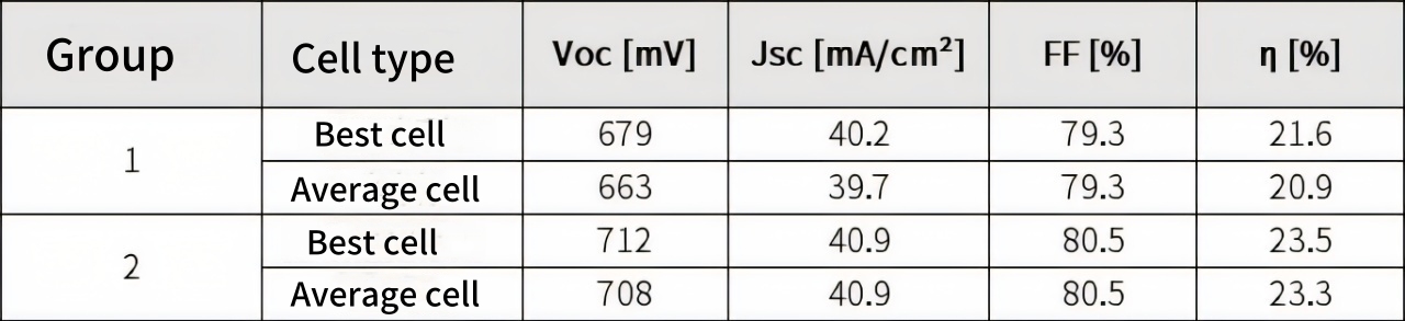
Comparison of I-V test results of two groups of solar cells
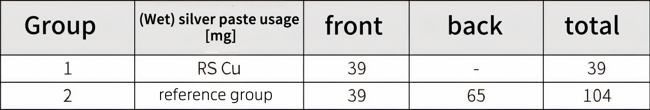 Wet silver paste deposition data for two groups of solar cells
Open circuit voltage (Voc): The average Voc of the experimental group is about 45 mV lower than that of the control group, which may be due to the fact that the back copper paste caused a certain degree of damage to the TOPCon passivation layer during the sintering process, resulting in an increase in carrier recombination losses.
Short circuit current density (Jsc): The Jsc of the experimental group is slightly lower than that of the control group, which is related to the decrease in Voc, which may be due to the increase in carrier recombination losses leading to a decrease in the number of photogenerated carriers.
Fill factor (FF): The FF of the experimental group is about 1.2% lower than that of the control group, indicating that there is a certain series resistance loss in the experimental group solar cell.
solar cell efficiency: The efficiency of the best solar cell in group 1 reached 21.6%, and the average efficiency was 20.9%; the efficiency of the best solar cell in group 2 was 23.5%, and the average efficiency was 23.3%.
The wet weight of the silver paste in the experimental group was reduced by about 65 mg, which is equivalent to a reduction of about 62% in the silver consumption per solar cell. Compared with the control group, the silver consumption of the experimental group was reduced from about 17 mg/W to about 7 mg/W.
Fabrication of large-size TOPCon solar cells by electroplating copper metallization
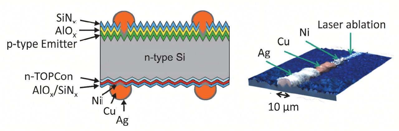
iTOPCon solar cell structure using electroplated nickel, copper and silver metallization process
Laser contact opening (LCO): Use picosecond pulse laser to locally open holes on the front and back passivation layers of the solar cell to form narrow finger-shaped openings for subsequent metallization. The width of the finger-shaped openings on the front is 5μm and on the back is 10μm.
Electroplating metallization: On the solar cell after LCO, a nickel diffusion barrier layer, a copper conductive layer, and a silver capping layer are deposited in sequence by electroplating. The nickel layer acts as a diffusion barrier to prevent copper from diffusing into silicon; the copper layer provides the main conductive function; and the silver layer is used to prevent copper oxidation and improve conductivity.
Grid layout: There are 194 finger lines and 12 pseudo busbars (20μm wide) on the front, and 235 finger lines and 12 pseudo busbars (50μm wide) on the back. This layout helps optimize the current collection and transmission efficiency of the solar cell.
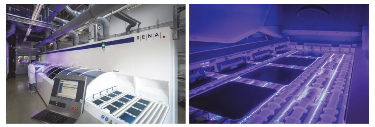
Electroplating production line
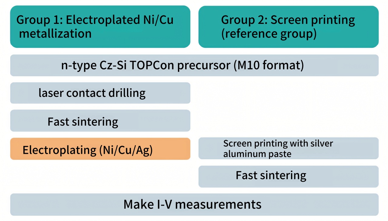 Flowchart of Experiment 2
The schematic diagram shows the entire process from cell substrate to metallization, including key steps such as passivation layer deposition, laser opening and electroplating metallization. This helps to understand how the electroplating Ni/Cu/Ag metallization process is used and implemented in iTOPCon solar cells.
Group 1 (electroplating Ni/Cu/Ag metallization):
Laser contact opening (LCO): Picosecond pulsed lasers are used to locally open holes in the front and back passivation layers of the cell to form narrow finger-shaped openings for subsequent metallization. The finger-shaped openings are 5μm wide on the front and 10μm on the back.
Electroplating metallization: On the cell after LCO, a nickel diffusion barrier layer, a copper conductive layer and a silver capping layer are deposited in sequence using the RENA InCellPlate electroplating line. The nickel layer prevents copper from diffusing into the silicon, the copper layer provides the main conductive function, and the silver layer is used to prevent copper oxidation and improve conductivity.
Group 2 (Silver Screen Printing Paste Metallization):
Front Metallization: Front side metallization with advanced AgAl screen printing paste, grid printing without busbars, 154 fingers, 24μm width.
Rear side metallization: Grid printing with silver paste, 198 fingers, 24μm width.
Experimental results of Experiment 2
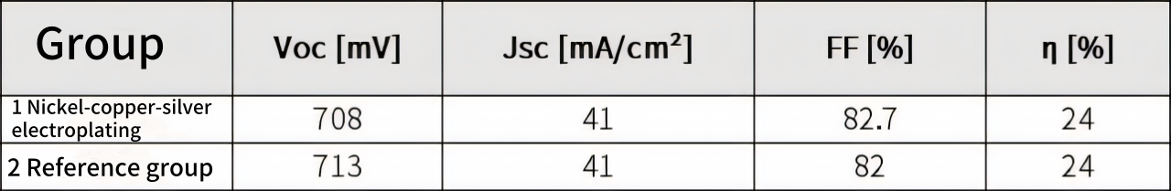 I-V measurement results of the two best solar cell groups
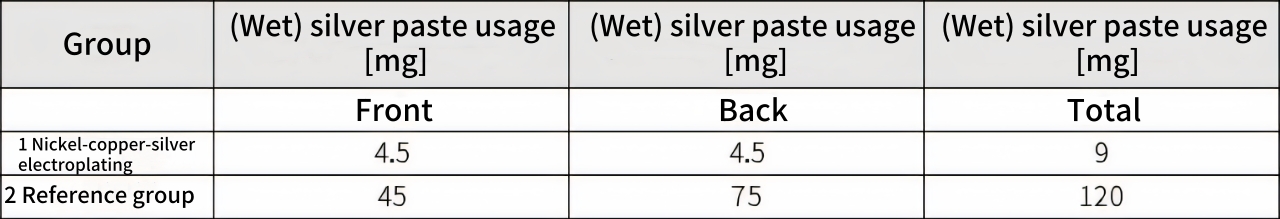 Estimated silver consumption for two solar cell groups
For the first time, the M10 large-size TOPCon solar cells were successfully prepared. The best cell efficiency of the electroplating group and the screen-printing reference group was 24.0%. The fill factor of the electroplating group was slightly higher, and the open-circuit voltage of the screen-printing group was slightly higher.
The electroplating group deposited only 9 mg of silver as a cover layer per cell, and the silver consumption was reduced to about 1 mg/W, which was about 93% less than the screen-printing reference group (about 15 mg/W). If tin or other materials were used to replace the silver cover layer, the use of silver could be completely avoided.
The electroplating nickel, copper and silver (Ni/Cu/Ag) metallization process not only successfully reduced the silver consumption to about 1 mg/W, which was about 93% less than the traditional screen-printing process, but also maintained the cell photoelectric conversion efficiency stable at 24.0%, showing its great potential in reducing production costs and improving the sustainability of the photovoltaic industry.


 English
 español
 한국의
한국의


 IPv6 network supported