

The world is working to improve the efficiency of perovskite photovoltaic cells, among which tandem solar cells (TSCs) have become a research hotspot due to their high efficiency, low heat loss and easy integration. This paper systematically analyzes the optimization path of double-sided perovskite/silicon tandem cells, focusing on the role of IBC structure and grating design in improving efficiency.
Solar cell structure and material selection
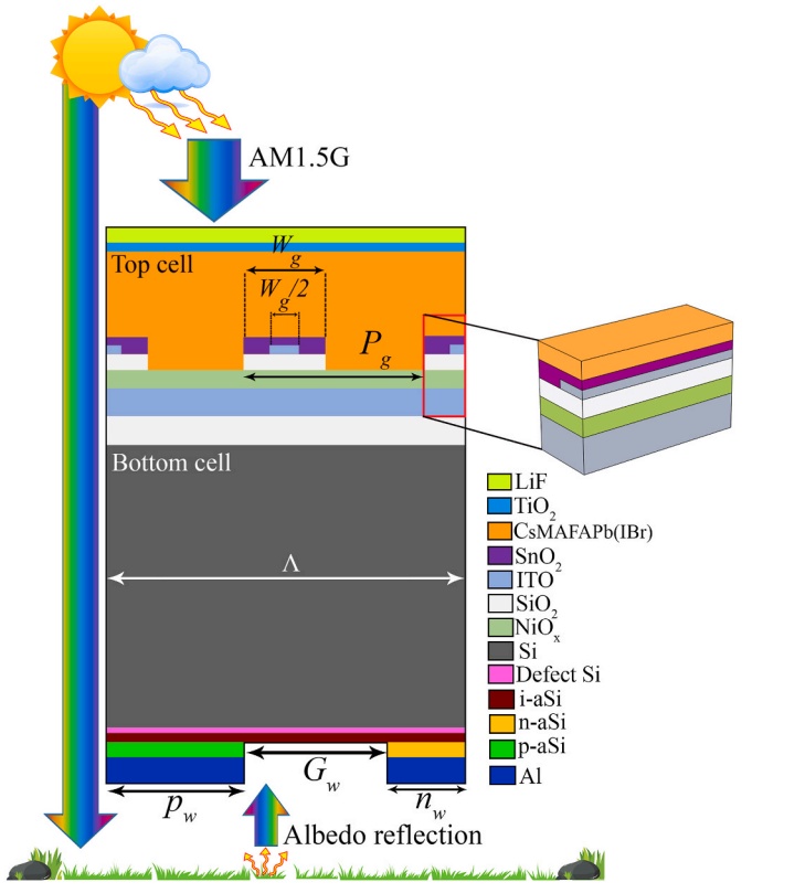
Schematic diagram of the structure of a four-terminal double-sided perovskite/crystalline silicon stacked solar cell under albedo reflection
Top perovskite cell:
Active layer: Cs₀.₀₅MA₀.₁₅FA₀.₈Pb(I₀.₈Br₀.₂)₃ (bandgap 1.62 eV)
Transport layer: SnO2 (ETL)/NiOX (HTL) combination, with low temperature process compatibility and high stability
Electrode: Double-sided ITO (30 nm cathode/200 nm anode)
Innovative design: IBC structure has both grating function (period Pg=700 nm, width Wg=350 nm)
Bottom silicon heterojunction cell:
Contact layer: 200 nm Al electrode (connecting n/p regions respectively)
Carrier selection layer: n-type aSi (20 nm, doped 1.5×1019cm-3) and p-type aSi (20 nm, doped 2×1019 cm-3)
Passivation layer: 5 nm intrinsic aSi (i-aSi)
Absorption layer: 300 μm n-type crystalline silicon (doped 5×1015cm-3)
Interface layer: 1 nm defective silicon (simulated interface recombination)
Intermediate connection layer:
Optical coupling layer: 150 nm SiO₂ (refractive index matching)
Electrical isolation layer: 50 nm SiO₂ (breakdown field strength>10 MV/cm)
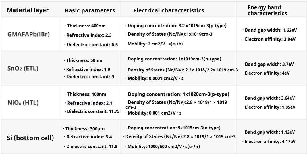
Photoelectric characteristic parameters of each layer of the cell
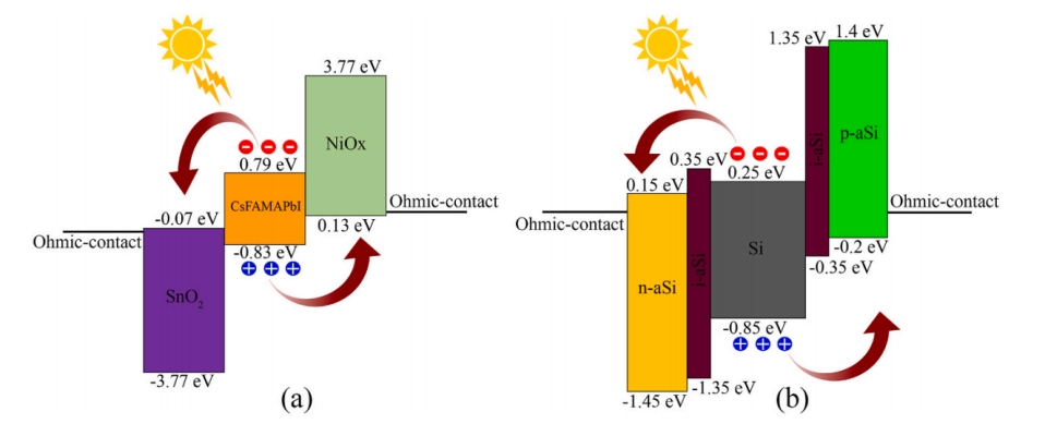
Schematic diagram of the energy band structure of the designed solar cell (a) top cell and (b) bottom cell
Simulation method and parameter setting
Optical simulation: The absorption characteristics in the wavelength range of 300–1200 nm are calculated using the finite difference time domain method (FDTD).
Carrier transport and recombination: Simulated by the drift-diffusion equation, the key parameters include:
Trap-assisted recombination: The carrier lifetime of the perovskite layer τₙ=τₚ=40ns (calculated based on Nₜ=1×1015cm-3 and σₙₚ=2.5×10⁻¹⁵ cm2).
Auger recombination: Perovskite Cₙ=Cₚ=4.4×10⁻²⁹cm6/s.
Radiative recombination: Perovskite Cᵣ=5.3×10⁻¹¹ cm3/s.
Albedo reflection simulation: Considering different ground types (asphalt, concrete, snow, etc.), the AM1.5G spectrum intensity is adjusted by a coefficient of 0.1–0.8.
Top cell anti-reflection layer (ARC) optimization
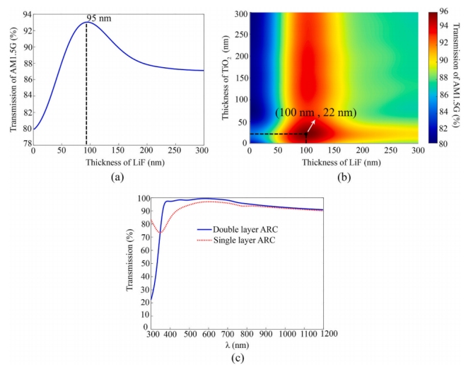 Transmission spectrum of the perovskite layer at the optimal thickness point
The double-layer ARC (LiF/TiO2) has a higher transmittance in the 350–800 nm band (96% vs. 93%).
Optimal thickness: LiF (100 nm)/TiO2 (22 nm).
Top cell back contact grating design
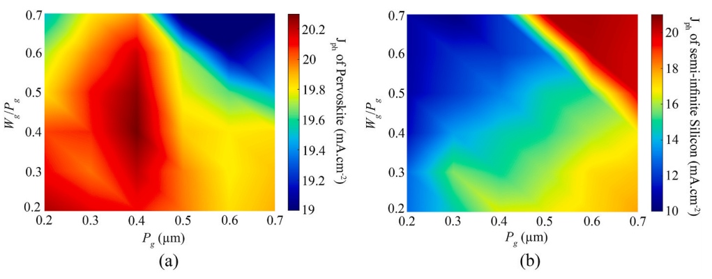
Relationship between photocurrent density (Jph) and top cell back contact grating period (Pg) and width-to-period ratio (Wg/Pg)
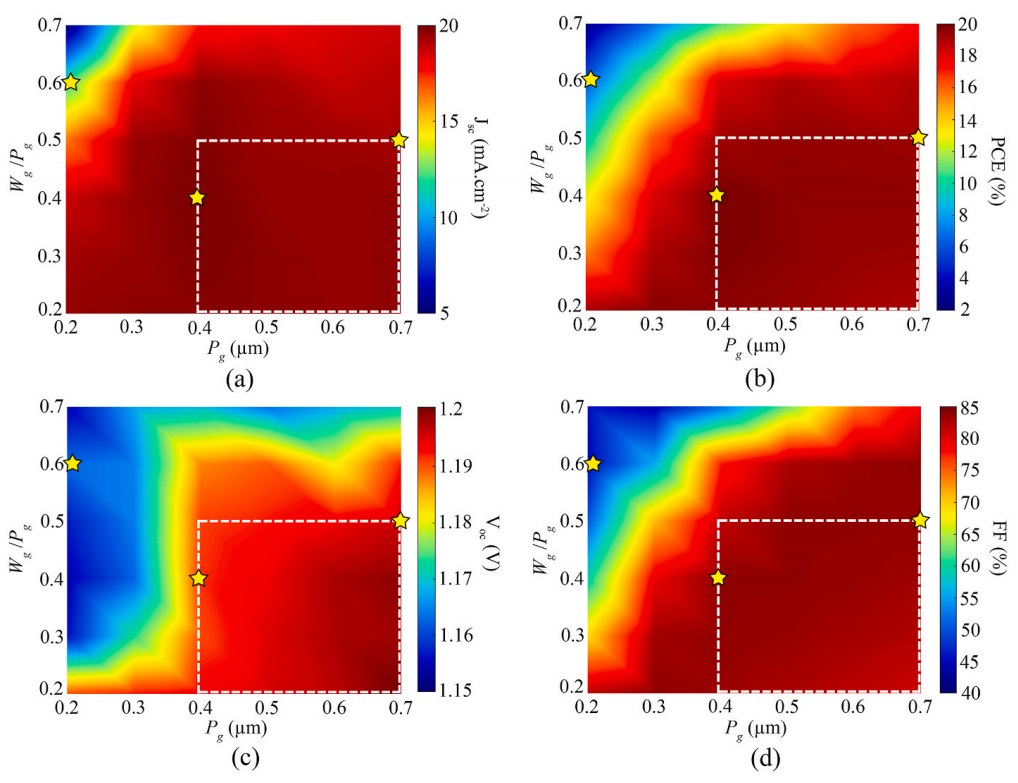
Color mapping of the top cell's (a) short-circuit current density (Jsc), (b) photoelectric conversion efficiency (PCE), (c) open-circuit voltage (Voc), and (d) fill factor (FF) as a function of the back contact grating period (Pg) and width-period ratio (Wg/Pg)
Optimal parameters: When Pg=0.4 μm and Wg/Pg=0.4, the top cell photocurrent (Jph) reaches 20.3 mA/cm².
Quasi-current matching: When Pg=0.7 μm and Wg/Pg=0.5, the top/bottom cell Jph is close (19.45/19.91 mA/cm²).
Top cell performance analysis
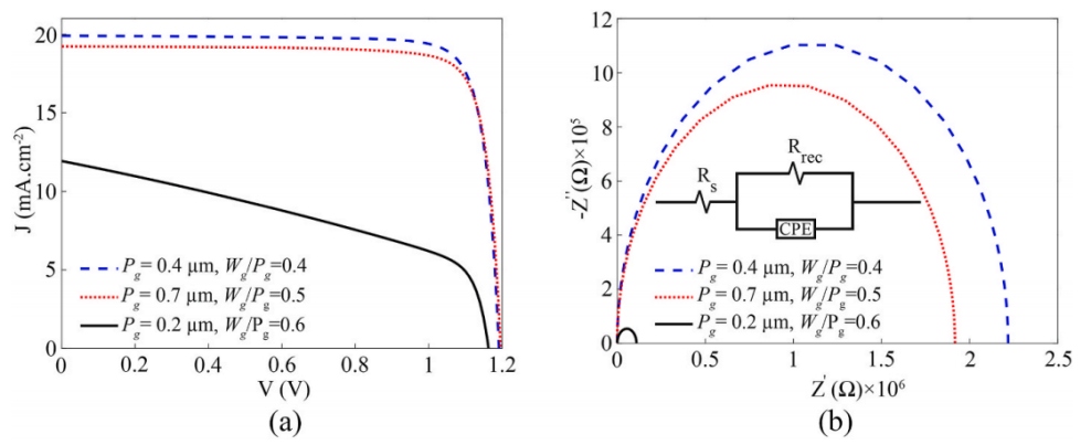
(a) Current density-voltage (J-V) characteristic curve of (Pg, Wg/Pg) parameter group;
(b) Nyquist plot of electrochemical impedance spectroscopy (EIS)
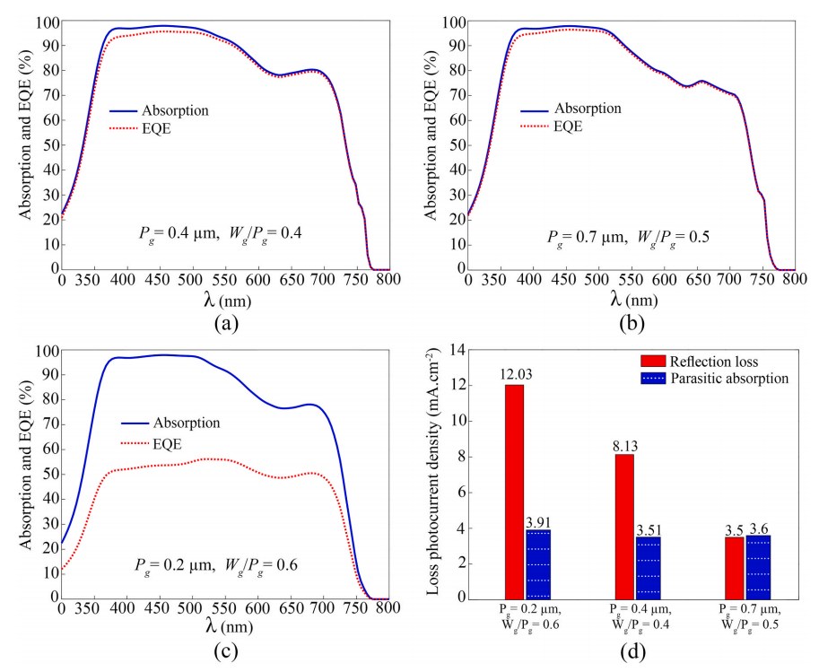 Absorption spectra and external quantum efficiency (EQE) spectra under different grating parameter combinations (Pg, Wg/Pg); (d) reflection and parasitic absorption photocurrent density losses of the corresponding parameter groups
Optimal structure (Pg=0.7 μm, Wg/Pg=0.5):
High composite resistance (Rrec=1.92 MΩ), low series resistance (Rs=12.95 Ω).
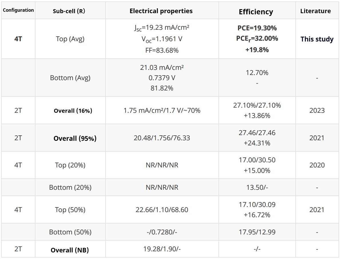
Highest open circuit voltage (Voc=1.196 V), PCE up to 19.3%.
Poor structure (Pg=0.2 μm, Wg/Pg=0.6): PCE only 6.23%, FF as low as 45%.
Bottom cell anti-reflection layer (ARC) optimization
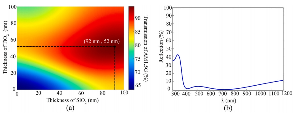
(a) Double-layer (SiO₂/TiO₂) structure;
(b) Reflection spectrum corresponding to the silicon layer surface
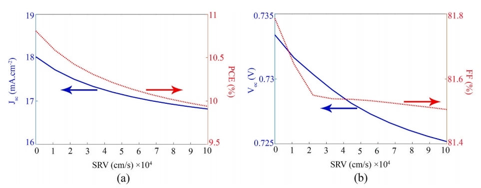 Curve of the influence of SRV on electrical parameters
The optimal thickness of double-layer ARC (SiO2/TiO2) is SiO2=92 nm, TiO2=52 nm, and the light transmission rate is increased to 94%.
Effect: PCE is increased to 10.81%, and Jsc is increased by 9%.
Bottom cell back contact grating design

Color mapping of fill factor (FF) with n-type amorphous silicon width (nw) and gap width (Gw)
Optimal parameters: nw=400 μm (20% of the period), Gw=1280 μm (80%).
Effect: PCE reaches 9.94% (Jsc=16.55 mA/cm², Voc=0.734 V).
Comparison: Too large nw (1600 μm) will reduce hole extraction, and PCE is only 7.14%.
Bottom cell performance analysis
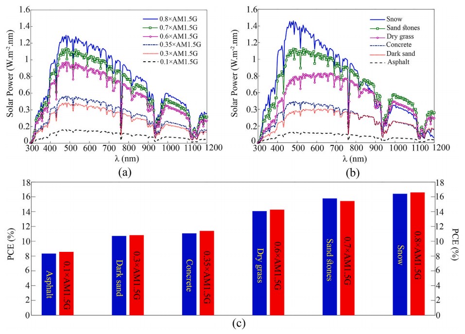
PCE comparison bar graph at different reflectivity
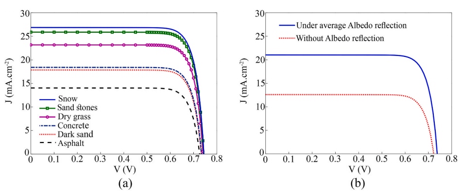 (a) Current density-voltage (J-V) characteristic curve under different albedo reflection conditions, (b) Comparison of J-V characteristic curves under average albedo and no albedo conditions
High reflection environment (such as 80% snow): PCE reaches 16.59%, which is 53% higher than asphalt (10% reflection).
Typical dark sand (30% reflection): Jsc and PCE are increased by 43% and 46% respectively compared with no reflection.
Best performance
 Top cell: The best combination of double-layer ARC + grating (Pg=0.7 μm, Wg/Pg=0.5), taking into account high light transmittance, low reflection (3.5 mA/cm² loss) and efficient charge collection.
Bottom cell: Through IBC geometry optimization (Gw maximization) and double-layer ARC, the PCE can reach 16.59% in highly reflective environments such as snow.
Total efficiency: After combining with the top cell, the total efficiency exceeds 30%, which is one of the highest levels of planar structure stacked cells.


 English
 español
 한국의
한국의


 IPv6 network supported