

Perovskite solar cells (PSCs) have become a research hotspot in the photovoltaic field due to their high efficiency and low cost, but their performance is limited by charge recombination and interface defects in the electron transport layer (ETL). SnO₂ is an ideal candidate material for ETL due to its high transmittance (>85%) and chemical stability, but its intrinsic defects (such as oxygen vacancies) limit its conductivity.
In this study, niobium-doped SnO₂ (SnO₂:Nb) thin films were prepared by atomic layer deposition (ALD) technology, and the transmittance of ETL was accurately characterized in real time by combining the Meineng perovskite online transmittance tester to ensure that its transmittance in the visible light range is >85%, thereby maximizing the light absorption efficiency of the perovskite layer (absorbance >90%).
Preparation of perovskite solar cells
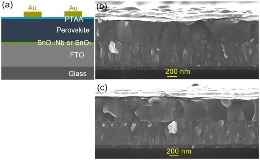
(a) Schematic diagram of n-i-p structure perovskite solar cell; (b) S₀ device (undoped SnO₂ ETL) and (c) O₅ device (Nb-doped SnO₂ ETL) cross-sectional SEM images
PSC cells adopt n-i-p structure, with FTO glass as substrate, and 15 nm SnO₂ : Nb or intrinsic SnO₂ thin film deposited by ALD at 100°C. Nb doping is achieved by adjusting the precursor pulse sequence (O sequence and S sequence) and cycle ratio (such as 55:1, 15:1, etc.), and the doping amount is determined by XPS depth profile analysis (0-3.45 at.%). The perovskite layer is Cs₀.₀₅ (MA₀.₁₆₆FA₀.₈₃₃) ₀.₉₅Pb (Br₀.₁₆₆I₀.₈₃₃)₃, deposited by anti-solvent assisted spin coating and annealed at 100°C. PTAA was then deposited as a hole transport layer (HTL), and the Au electrode was prepared by thermal evaporation.
Electrical performance test and analysis
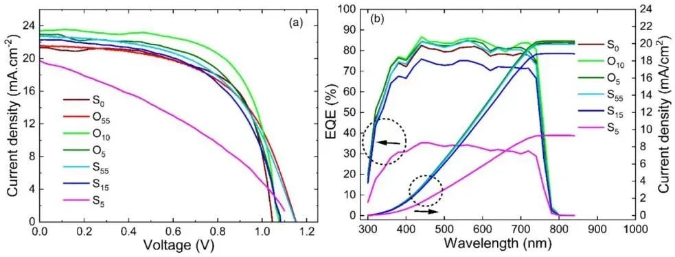
(a) Current density-voltage (J-V) curves of PSC cells based on SnO₂:Nb and undoped SnO₂ ETL in the reverse scanning direction; (b) Changes in external quantum efficiency (EQE) and integrated current density with wavelength
The PCE of the intrinsic SnO₂ ETL device (S₀) is 12.15%, while the PCE of the optimal SnO₂:Nb ETL device (O₁₀) reaches 13.08%, an efficiency improvement of 7.65%, mainly attributed to the improvement of Voc (1.05→1.06 V) and Jsc (18.81 → 20.34 mA/cm²).
Low-doping (≤0.2 at.%) devices (such as O₅₅, O₁₀) significantly optimize the charge transfer efficiency due to the reduction of series resistance (Rₛ=48.35 Ω·cm² vs. 62.10 Ω·cm² of S₀) and the increase of parallel resistance (Rₛₕ=12.77 Ω·cm² vs. 5.32 Ω·cm² of S₀). High-doping (>0.2 at.%) devices (such as S₅, Nb=3.45 at.%) have a sudden drop in FF to 32.70% (Rₛ=443.67 Ω·cm²), resulting in a drop in PCE to 6.12%, indicating that excessive doping introduces interface resistance and defects.
Study on the characteristics of perovskite layer
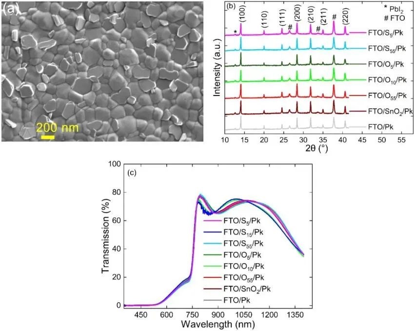
(a) Top view SEM image of FTO/O₁₀/Pk half-cell; (b) XRD patterns of perovskite layers with different ETLs; (c) Optical transmission spectra of perovskite layers
XRD and SEM show that all perovskite layers on ETLs present dense grains (size 60–70 nm) and (100) preferred orientation, and PbI₂ impurities are not enriched at the interface, proving that ETL modification does not affect the crystallinity of perovskites.
The light absorption characteristics of the perovskite layer directly affect the efficiency of the solar spectrum utilization of the solar cell. The analysis of UV-Vis-NIR transmission and absorption spectra revealed that:
Absorption edge position: All samples show obvious absorption edges at 765 nm, corresponding to an optical band gap (Eg) of 1.62 eV. This is consistent with the typical band gap of ternary cation perovskites, indicating that Nb doping does not change the bulk optical properties of perovskites.
Absorbance and transmittance: In the visible light range (400–750 nm), the absorbance of the perovskite layer exceeds 90%, while the transmittance of SnO₂ or SnO₂:Nb ETL is >85%, indicating that the high transparency of the ETL ensures that the incident light is fully absorbed by the perovskite layer, reducing optical losses.
Carrier dynamics and band engineering
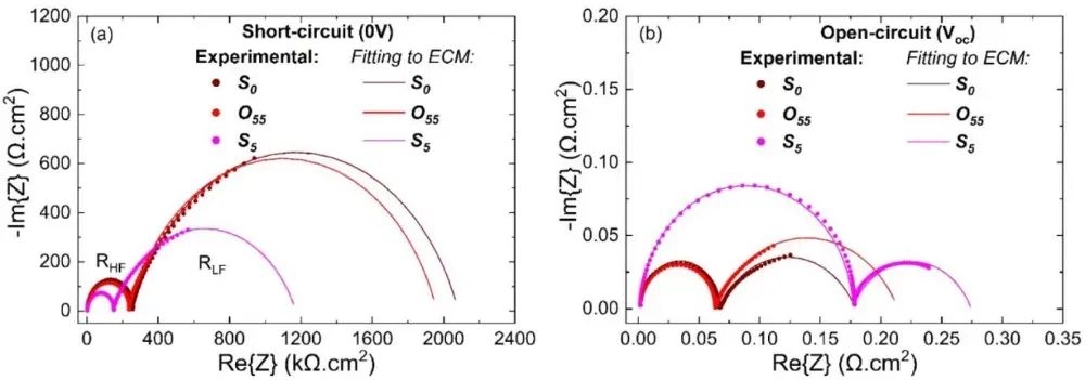
Impedance spectrum of PSC cell under illumination (Nyquist plot): (a) short-circuit condition (V_DC=0 V); (b) open-circuit condition (V_DC=Vₒc)
Impedance spectrum analysis: The series resistance (Rₛ=48.35 Ω·cm²) of low Nb-doped device (O₁₀) is lower than that of undoped S₀ (62.10 Ω·cm²), indicating that the carrier transfer efficiency is improved.
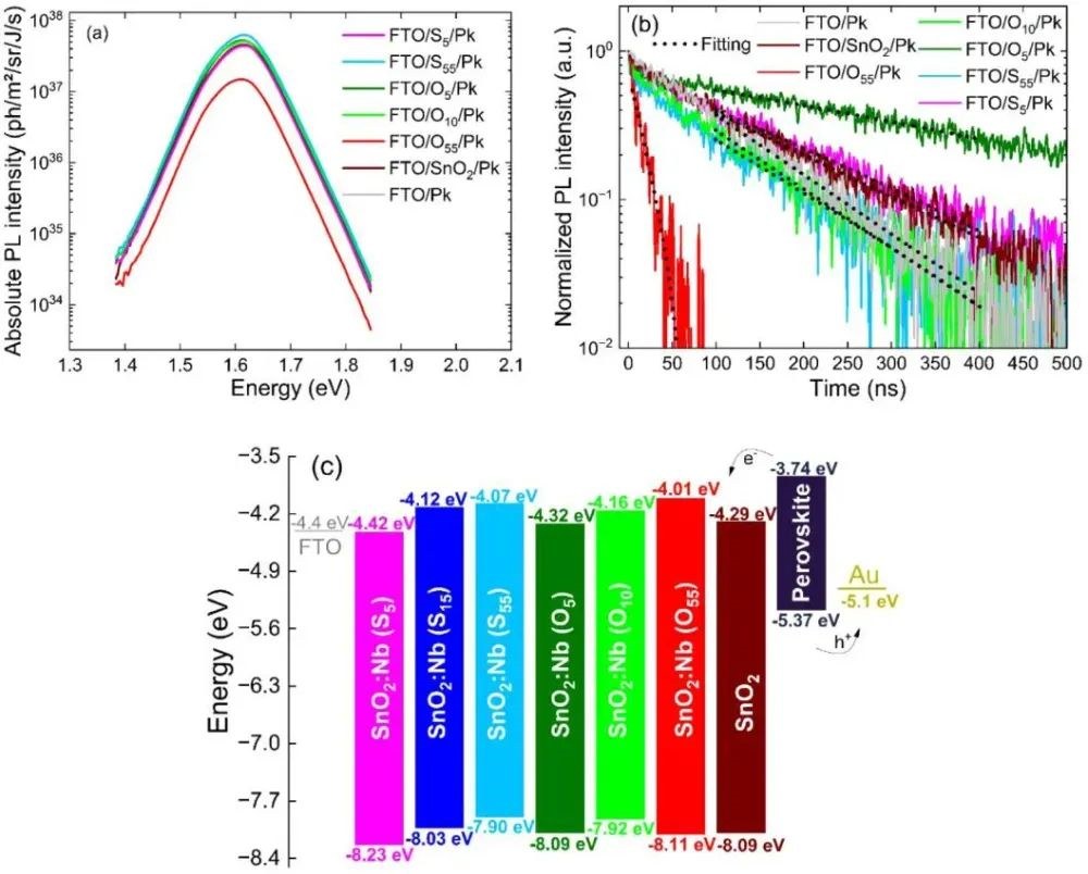
(a) Steady-state photoluminescence (PL) spectrum; (b) Transient photoluminescence (TRPL) decay curve; (c) Energy band diagram of perovskite, SnO₂ and SnO₂:Nb ETL
TRPL decay: The carrier lifetime of O₁₀ device (τ=461 ns) is significantly higher than that of S₀ (149 ns), indicating that the interface non-radiative recombination is reduced.
Band alignment: Nb doping makes the SnO₂ conduction band close to the perovskite conduction band, reducing the electron extraction barrier and inhibiting the interface charge accumulation.
In this study, the conductivity and band matching of SnO₂:Nb ETL can be significantly improved by precisely controlling the Nb doping concentration (≤0.2 at.%) through atomic layer deposition (ALD) technology, thereby optimizing the photovoltaic performance of perovskite solar cells (PSCs). The study further revealed that the high transmittance of SnO₂:Nb ETL (transmittance > 85%) ensures that the perovskite layer fully absorbs the incident light (absorbance > 90%), effectively reducing optical losses.


 English
 español
 한국의
한국의


 IPv6 network supported