

Perovskite solar cells have achieved laboratory efficiencies exceeding 25%, but commercialization faces three major challenges: long-term stability, toxicity, and the process of scaling up to industrial-related areas. However, in the process of scaling up from laboratory cells (<0.1 cm²) to industrial-grade modules (>100 cm²), uniform deposition and low-loss interconnection are two core challenges. Traditional solution methods (such as blade coating and slit coating) significantly degrade in performance during scale-up due to solvent evaporation and complex crystallization dynamics, while vapor deposition techniques (such as co-evaporation) are considered to be an effective way to achieve uniform large-area deposition.
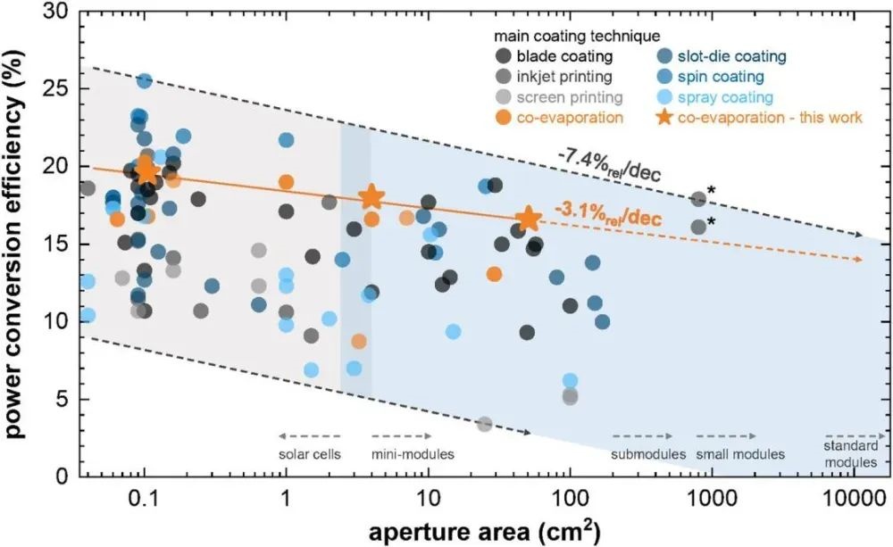
Relationship between efficiency and area of different deposition technologies
When the solution method is scaled up, the PCE loss is significant (e.g., the area loses 19.7% when it goes from 0.8 to 42.9 cm²), and the average scale-up loss is 7.4%/dec.
The full evaporation + laser scribing technology in this study loses only 3.1%/dec when it goes from 4 to 51 cm², which is close to traditional thin film technology (such as CIGS, c-Si, CdTe). Using the Menon Perovskite P1 laser scribing tester for full laser scribing can achieve high-precision interconnection (total width ≤ 160 μm).
Full evaporation layer manufacturing and full laser etching interconnection
Full evaporation layer preparation
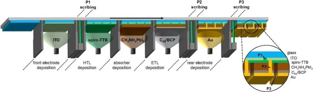
Preparation process and layer structure of fully evaporated perovskite components
Process diagram:
■ Glass substrate → ITO deposition → P1 scribing (isolate front electrode).
■ Hole transport layer (spiro-TTB) → Perovskite absorption layer (co-evaporation) → Electron transport layer (C60/BCP) → Back electrode (Au/Ag).
■ P2 scribing (connecting back electrode and front electrode) → P3 scribing (isolating back electrode)
■ Full vacuum deposition avoids solvent interference of solution method, and laser scribing is a non-contact process, which is compatible with large-scale production. The laser system ensures that the environment is controllable (nitrogen protection) to reduce perovskite oxidation or water absorption.
▶ Full laser scribing interconnection technology
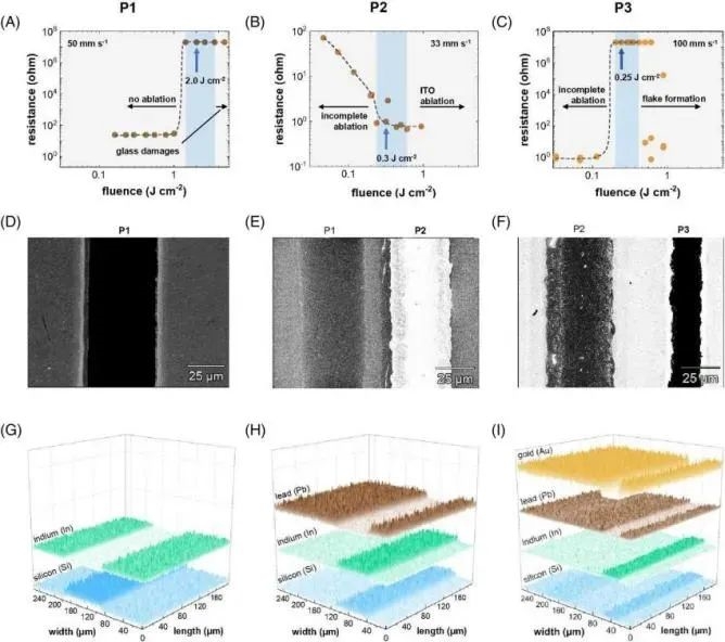
Laser Scribing Parameter Optimization and Morphology Analysis
Use 532 nm nanosecond laser to complete P1 (isolated front electrode), P2 (connected front and rear electrodes), P3 (isolated rear electrode) etching:
P1: energy density 2 J·cm⁻², speed 50 mm/s, line width 60 μm;
P2: energy density 0.35 J·cm⁻², speed 33 mm/s, line width 50 μm, contact resistance <1 Ω;
P3: energy density 0.3 J·cm⁻², speed 100 mm/s, line width 25 μm.
Performance verification:
Electrical characteristics: SEM-EDX shows that the P2 line completely removes ETL/perovskite/HTL, and the residual lead signal is <1%;
Geometric fill factor (GFF): 4 cm² component GFF=96%, 51 cm² component GFF=94%, better than the solution method (GFF≈85%);
Production compatibility: The single laser source process simplifies the complexity of the equipment, and the etching speed (up to 100 mm/s) supports mass production cycles >1 piece/minute.
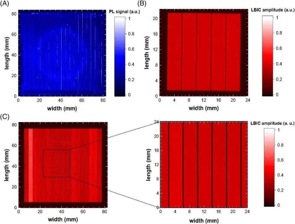
(A) PL imaging of 51 cm² perovskite absorption layer; (B) 4 cm² module LBIC; (C) 51 cm² module LBIC and local magnification
Uniformity: PL imaging shows that the luminescence intensity fluctuation of the 51 cm² perovskite layer is <5%, the signal is uniform, and the edge effect is minimal;
4 cm² module: the current signal is uniform, confirming the interlayer uniformity and low contact resistance.
51 cm² module: the signal decreases slightly (GFF from 96% → 94%), but it is still better than most solution-based modules.
The full evaporation process achieves large-area uniform deposition, and laser scribing does not introduce significant defects.
Perovskite module performance and loss analysis
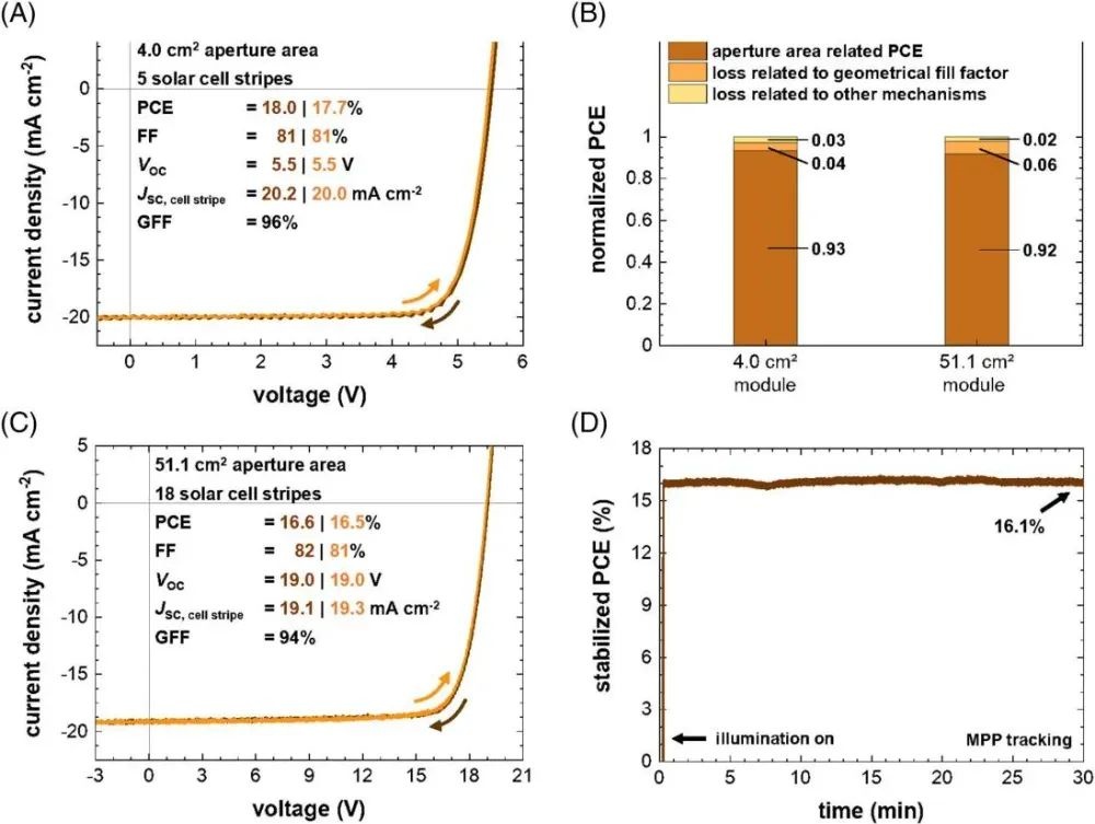
(A) 4 cm² module PCE; (C) 51 cm² module PCE; (B) Scaled loss; (D) 51 cm² module MPP tracking
4 cm² module: PCE=18.0% (backward scan), FF=81%, Voc=5.5 V, Jsc=20.2 mA/cm².
51 cm² module: PCE=16.6% (backward scan), FF=82%, Voc=19.0 V, Jsc=19.1 mA/cm².
Loss analysis: Of the total loss of 3.1%/dec from 4→51 cm², GFF contributes 2.2%, and other mechanisms (such as resistance, defects) only 0.9%. The stability of the 51 cm² module under MPP tracking, the efficiency maintained at 16.1% within 30 minutes.
The fully evaporated module remains efficient and stable over a large area.
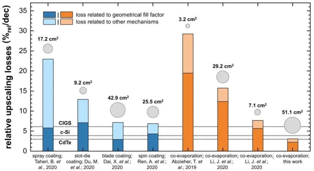
Comparison of amplification losses of different technologies
■ Solution method (such as blade coating, slit coating) loses 6.9–7.2%/dec.
■ Full evaporation + laser scribing loses 3.1%/dec, which is close to traditional technologies such as CIGS (~3%) and c-Si (~2%).
■ Vapor deposition combined with laser scribing is currently the technical path with the lowest efficiency loss in perovskite amplification.
This study successfully achieved efficient large-scale amplification of perovskite components through the synergy of full evaporation layer manufacturing and full laser scribing. The full vacuum deposition process solves the problem of large-area uniformity, while single-source nanosecond laser scribing simplifies the interconnection process and reduces resistance loss. The resulting component still maintains an efficiency of 16.6% at an area of 51 cm², with an amplification loss of only 3.1%/dec, marking an important step for perovskite photovoltaics towards industrialization.


 English
 español
 한국의
한국의


 IPv6 network supported