

1. XBC solar cell technology
(1) BC is not a completely new solar cell technology
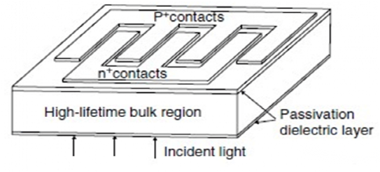
Back Contact, metal electrodes are arranged on the back of the solar cell in a cross-finger shape, creating more light-absorbing area for the front and improving the overall photoelectric conversion efficiency of the cell.
(2) BC is not an isolated solar cell technology
TBC=TOPCon (tunneled silica/doped polysilicon) + BC (full backside contact); HBC = HJT (non/microcrystalline silicon) + BC (full backside contact), TBC/HBC competition is essentially a further differentiated competition between TOPCon and HJT.
(3) BC has high technical barriers, and it is not possible to switch to BC solar cells at any time with TOPCon/HJT reserves
a. The production process of BC solar cell is long, especially the back electrode production is more cumbersome, and it needs to go through 2~3 laser slotting processes, which requires high equipment stability/process maturity level, and the leakage problem caused by the laser grooving process is an important bottleneck restricting the yield of cell production;
b. Since the back electrodes cross each other, the solder strip design/soldering process and packaging process also need to be adjusted accordingly. In terms of welding strips, the trend of flattening, thinning and widening; In terms of adhesive film, the mainstream scheme EPE+POE, the thickness of the adhesive film can decrease with the ultra-thin welding tape; In terms of stringer welding machine, the welding accuracy requirements have been greatly improved, and a BC special stringer is required.
(4) BC technology is highly suitable for electroplating copper. In the current metallization scheme, electroplated copper and silver paste have their own advantages, and in the long run, for BC solar cells with complex processes and high manpower, equipment and material costs, electroplated copper shows great potential in cost and process matching.
2. XBC solar cell structure
(1) BC solar cell infrastructure
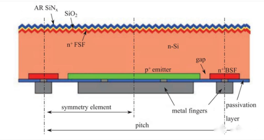
a. From top to bottom: SiNx/SiO2-n+Si (phosphorus-doped)-Si substrate-p+ (boron expansion)/n++ (phosphorus expansion)Si-SiO2/SiNx - metal electrode (interphalangely)
b. n+Si (phosphorus-doped): The field passivation effect is used to reduce the surface oligo concentration, thereby reducing the surface recombination rate, while also reducing the series resistance and improving the electron transport capacity.
c. p+Si (boron amplification): The emitter can form a p-n junction with the N-type silicon substrate to effectively shunt carriers.
d. n++Si (phosphorus expansion): forming a high and low junction with n-type silicon to enhance the separation ability of carriers is the core technology of IBC solar cells.
e. SiO2/SiNx: backside, inhibition of carrier recombination of IBC solar cells; On the front side, the anti-reflection layer improves the efficiency of power generation.
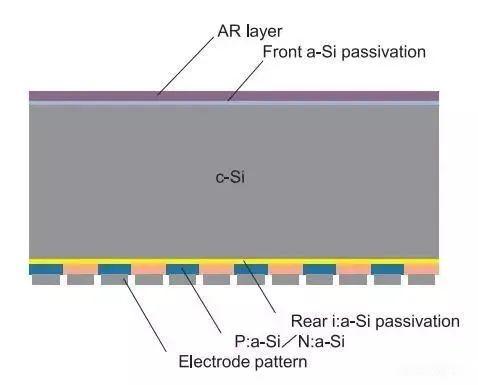
(2) HBC solar cell structure (HJT/BC)
From top to bottom: anti-reflection layer-intrinsic amorphous silicon-Si substrate-intrinsic amorphous silicon-n/p-type amorphous silicon-TCO-metal electrode
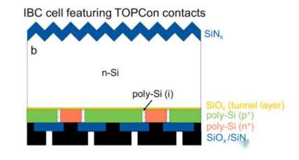
(3) TBC structure (TOPCon/BC)
From top to bottom: anti-reflection layer - passivation layer - AlOx-n+Si (phosphorus-doped) - Si substrate - tunneling oxide layer - p+/n++ doped polysilicon - passivation layer - anti-reflection layer - metal electrode
3. XBC solar cell process
| IBC | TBC | HBC | |
| 1 | Cleaning and texturing | Cleaning and texturing | Cleaning and texturing |
| 2 | Phosphorus diffusion | Tunneling oxide layer + n-type amorphous silicon | Intrinsic hydrogenated amorphous silicon (front) |
| 3 | Masking | Masking | Anti-reflective coating (front) |
| 4 | Laser grooving | Laser grooving | Intrinsic hydrogenated amorphous silicon (back) |
| 5 | Etching | Boron-doped amorphous silicon (P+) | Boron-doped amorphous silicon (P+) |
| 6 | Clean the mask | Etching | Masking |
| 7 | Double-sided anti-reflection + passivation | Double-sided anti-reflection + passivation | Laser grooving |
| 8 | Laser grooving (PERC) | Laser slotting (P/N separation) | Etching |
| 9 | Metallization | Metallization | Phosphorus-doped amorphous silicon (back) n++ |
| 10 | Transparent conductive film (back) | ||
| 11 | Laser grooving (P/N separation) | ||
| 12 | Metallization |


 English
 español
 한국의
한국의


 IPv6 network supported